16
LTC1421/LTC1421-2.5
APPLICATIONS INFORMATION
U
U
U
V
CCLO
1
2
3
4
V
CCHI
DISABLE
CON1
CON2
CPON
PWRGD
V
TH2
1421 F17
V
OUTHI
GATEHI
GATELO
V
OUTLO
RESET
FAULT
POR
32祍
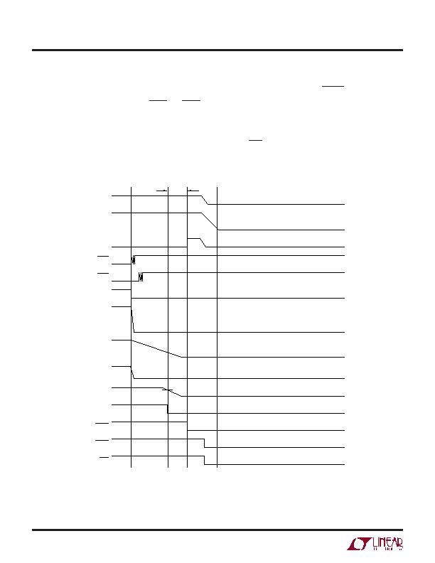
Figure 17. Board Removal Timing
Board Removal Timing
When the board is removed from the host, the sequence
happens in reverse (Figure 17). Since CON1 and CON2 are
the shortest pins, they break connection first and are
internally pulled high (time point 1). The charge pumps are
turned off, CPON is pulled low. V
OUTLO
and V
OUTHI
are
actively pulled down. When V
OUTLO
falls below its reset
threshold (time point 2) PWRGD is pulled low. To allow
time for power fail information to be stored in nonvolatile
memory, the falling edge of RESET (time point 3) is
delayed by 32祍 from the falling edged of PWRGD.
Finally, the input supply pins V
CCHI
and V
CCLO
break
contact (time point 4). If staggered pins are not used, the
board may be powered down prior to removal by switch-
ing the POR pin to ground with a toggle switch.
发布紧急采购,3分钟左右您将得到回复。
相关PDF资料
LTC1422CN8
IC CONTROLLER HOT SWAP 8-DIP
LTC1642CGN#TRPBF
IC CONTROLLER HOTSWAP ADJ 16SSOP
LTC1643AL-1CGN#PBF
IC CTRLR HOTSWAP PCI BUS 16SSOP
LTC1644CGN#TRPBF
IC CONTROLLER HOT SWAP 20-SSOP
LTC1645IS#TRPBF
IC CTRLR SEQ HOTSWAP DUAL 14SOIC
LTC1646IGN#TR
IC CNTRLR HOTSWAP PCIDUAL 16SSOP
LTC1647-1IS8#TRPBF
IC CONTROLLR HOTSWAP DUAL 8-SOIC
LTC1704EGN#TRPBF
IC REG DL BUCK/LINEAR 16SSOP
相关代理商/技术参数
LTC1421ISW-2.5#TR
功能描述:IC CONTROLLER HOTSWP 2.5V 24SOIC RoHS:否 类别:集成电路 (IC) >> PMIC - 热交换 系列:- 产品培训模块:Lead (SnPb) Finish for COTS
Obsolescence Mitigation Program 标准包装:119 系列:- 类型:热交换控制器 应用:通用型,PCI Express? 内部开关:无 电流限制:- 电源电压:3.3V,12V 工作温度:-40°C ~ 85°C 安装类型:表面贴装 封装/外壳:80-TQFP 供应商设备封装:80-TQFP(12x12) 包装:托盘 产品目录页面:1423 (CN2011-ZH PDF)
LTC1421ISW-2.5#TRPBF
功能描述:IC CONTROLLER HOT SWAP 24-SOIC RoHS:是 类别:集成电路 (IC) >> PMIC - 热交换 系列:- 产品培训模块:Obsolescence Mitigation Program 标准包装:100 系列:- 类型:热插拔开关 应用:通用 内部开关:是 电流限制:可调 电源电压:9 V ~ 13.2 V 工作温度:-40°C ~ 150°C 安装类型:表面贴装 封装/外壳:10-WFDFN 裸露焊盘 供应商设备封装:10-TDFN-EP(3x3) 包装:管件
LTC1422CN8
功能描述:IC CONTROLLER HOT SWAP 8-DIP RoHS:否 类别:集成电路 (IC) >> PMIC - 热交换 系列:- 产品培训模块:Obsolescence Mitigation Program 标准包装:100 系列:- 类型:热插拔开关 应用:通用 内部开关:是 电流限制:可调 电源电压:9 V ~ 13.2 V 工作温度:-40°C ~ 150°C 安装类型:表面贴装 封装/外壳:10-WFDFN 裸露焊盘 供应商设备封装:10-TDFN-EP(3x3) 包装:管件
LTC1422CN8#PBF
功能描述:IC CONTROLLER HOT SWAP 8-DIP RoHS:是 类别:集成电路 (IC) >> PMIC - 热交换 系列:- 标准包装:50 系列:- 类型:热交换控制器 应用:-48V 远程电力系统,AdvancedTCA ? 系统,高可用性 内部开关:无 电流限制:可调 电源电压:11.5 V ~ 14.5 V 工作温度:-40°C ~ 85°C 安装类型:表面贴装 封装/外壳:10-TFSOP,10-MSOP(0.118",3.00mm 宽) 供应商设备封装:10-MSOP 包装:管件
LTC1422CS8
功能描述:IC CONTROLLER HOT SWAP 8-SOIC RoHS:否 类别:集成电路 (IC) >> PMIC - 热交换 系列:- 标准包装:50 系列:- 类型:热交换控制器 应用:-48V 远程电力系统,AdvancedTCA ? 系统,高可用性 内部开关:无 电流限制:可调 电源电压:11.5 V ~ 14.5 V 工作温度:-40°C ~ 85°C 安装类型:表面贴装 封装/外壳:10-TFSOP,10-MSOP(0.118",3.00mm 宽) 供应商设备封装:10-MSOP 包装:管件
LTC1422CS8#PBF
功能描述:IC CONTROLLER HOT SWAP 8-SOIC RoHS:是 类别:集成电路 (IC) >> PMIC - 热交换 系列:- 产品培训模块:Lead (SnPb) Finish for COTS
Obsolescence Mitigation Program 标准包装:119 系列:- 类型:热交换控制器 应用:通用型,PCI Express? 内部开关:无 电流限制:- 电源电压:3.3V,12V 工作温度:-40°C ~ 85°C 安装类型:表面贴装 封装/外壳:80-TQFP 供应商设备封装:80-TQFP(12x12) 包装:托盘 产品目录页面:1423 (CN2011-ZH PDF)
LTC1422CS8#TR
功能描述:IC CONTROLLER HOTSWAP 8SOIC RoHS:否 类别:集成电路 (IC) >> PMIC - 热交换 系列:- 产品培训模块:Obsolescence Mitigation Program 标准包装:100 系列:- 类型:热插拔开关 应用:通用 内部开关:是 电流限制:可调 电源电压:9 V ~ 13.2 V 工作温度:-40°C ~ 150°C 安装类型:表面贴装 封装/外壳:10-WFDFN 裸露焊盘 供应商设备封装:10-TDFN-EP(3x3) 包装:管件
LTC1422CS8#TRPBF
功能描述:IC CONTROLLER HOT SWAP 8-SOIC RoHS:是 类别:集成电路 (IC) >> PMIC - 热交换 系列:- 产品培训模块:Obsolescence Mitigation Program 标准包装:100 系列:- 类型:热插拔开关 应用:通用 内部开关:是 电流限制:可调 电源电压:9 V ~ 13.2 V 工作温度:-40°C ~ 150°C 安装类型:表面贴装 封装/外壳:10-WFDFN 裸露焊盘 供应商设备封装:10-TDFN-EP(3x3) 包装:管件
